
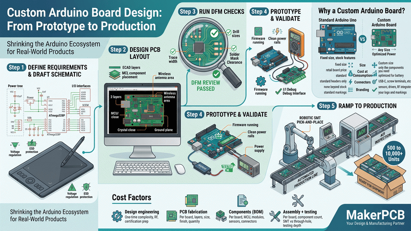
Designing a custom Arduino board allows you to take a working breadboard proof-of-concept and transform it into a compact, cost-effective, commercial-grade hardware product. By stripping away redundant peripherals found on off-the-shelf development boards (like the Uno or Mega) and integrating your exact interfaces, you significantly lower unit costs, optimize power consumption, and fit your product into custom enclosures.
This guide outlines the 5-step engineering process, cost breakdowns, manufacturing best practices, and key considerations for scaling your custom Arduino PCB design from prototype to full turnkey production.
What Is a Custom Arduino Board?
A custom Arduino board (or Arduino-compatible PCB) is an application-specific printed circuit board built around an Arduino-supported microcontroller (such as the Microchip ATmega328P, ATmega2560, or modern 32-bit ARM/ESP32 architectures).
It retains full compatibility with the Arduino IDE, standard bootloaders, and software libraries, but features a custom form factor, dedicated onboard peripherals (sensors, motor drivers, wireless modules), and tailored power management.
Common Commercial Applications:
• IoT & Environmental Monitoring: Low-power battery-operated sensor nodes.
• Robotics & Motion Control: Integrated motor drivers and encoder interfaces.
• Industrial Automation: 24V inputs, optocouplers, and RS-485 / CAN bus interfaces.
• Consumer Electronics & Smart Home: Form-factor constrained devices with integrated USB-C charging.
Standard Arduino Uno vs. Custom Arduino PCB
While a development board is ideal for bench testing, commercial deployment requires custom hardware.
| Feature / Factor | Standard Arduino Uno R3 | Custom Arduino PCB |
| Form Factor & Size | Fixed 68.6 × 53.4 mm | Any custom shape/size fitting your enclosure |
| Unit BOM Cost at Scale | 25 (retail overhead) | 10 (only components you need) |
| Power Optimization | High quiescent current (linear regulators, active LEDs) | Ultra-low deep-sleep modes (<10µA), optimized PMIC |
| Interface & Connectors | 2.54 mm female headers | USB-C, screw terminals, JST, latching connectors |
| Integrated Hardware | Basic MCU break-out | Onboard sensors, RF (Wi-Fi/BLE), relay drivers |
| Branding & Certification | Generic Arduino branding | Custom silkscreen, logos, FCC/CE pre-compliance layout |
5-Step Custom Arduino Design & Manufacturing Workflow
Step 1: Schematic Capture & Architecture Design
Define the core electrical specifications before launching CAD tools:
• Microcontroller Selection: ATmega328P (8-bit basic), SAMD21 (32-bit ARM Cortex-M0+), or ESP32 (integrated Wi-Fi/Bluetooth).
• Power Architecture: Determine input sources (LiPo battery, 12V/24V DC, or 5V USB-C) and choose appropriate LDOs or buck converters.
• Protection Circuits: Add TVS diodes for ESD protection, reverse-polarity protection (P-channel MOSFET/Schottky diode), and decoupling capacitors close to all VCC/AVCC pins.
Step 2: PCB Layout & High-Speed Routing
Transfer your schematic to an ECAD suite (Altium Designer, KiCad, or EasyEDA):
• Layer Count: Use a 2-layer PCB for standard low-speed designs; upgrade to a 4-layer stackup (Signal-GND-Power-Signal) for high-density routing, RF modules, or improved EMI performance.
• Component Placement: Keep the crystal oscillator as close to the MCU pins as possible with a surrounding ground loop.
• Grounding: Maintain an unbroken ground plane under critical high-speed lines (SPI, I2C, USB) to minimize return path inductance.
Step 3: Design for Manufacturing (DFM) Review
Before submitting orders to the fab house, verify board constraints to avoid costly revisions:
• Check minimum trace width and clearance (e.g., 5/5 mil or 6/6 mil).
• Confirm annular ring sizes, drill aspect ratios, and solder mask expansion.
• Ensure clear component clearance for automated SMT placement nozzles.
Step 4: Rapid Prototyping & Bring-Up (5–50 Units)
Order a quick-turn PCB assembly (PCBA) batch to validate hardware and firmware:
• Power Rail Bring-Up: Check 3.3V/5V rails with a multimeter before burning the bootloader.
• Bootloader Flashing: Burn the Arduino Optiboot bootloader via ICSP (In-Circuit Serial Programming) using an ISP programmer or another Arduino.
• Functional Validation: Verify peripheral communication (UART, I2C, SPI) and thermal behavior under load.
Step 5: Mass Production & Functional Testing (FCT)
Transitioning to batch manufacturing (1,000+ units) requires production-grade tooling:
• Automated Assembly: Surface Mount Technology (SMT) with automated optical inspection (AOI) and X-ray inspection (for BGA/QFN packages).
• Test Jigs: Bed-of-nails test fixtures to flash firmware and execute automated functional testing (FCT) in seconds per board.
Cost Breakdown: Custom Arduino PCB Manufacturing
The overall cost includes one-time engineering (NRE) and per-unit production costs:
| Cost Item | Estimated Budget | Key Cost Drivers |
| Hardware Engineering (NRE) | 4,000+ | Schematic complexity, custom RF, certification layout |
| Bare PCB Fabrication | 5.00 / board | Layer count (2 vs. 4+ layers), dimensions, surface finish (HASL vs. ENIG) |
| BOM / Components | 20.00 / board | MCU selection, specialized ICs, integrated wireless modules |
| SMT Assembly & Testing | 6.00 / board | SMT component count, through-hole soldering, custom test fixtures |
Choosing Between Arduino-Compatible vs. Pure Embedded C/C++ Design
• Keep Arduino Compatibility if: You want rapid prototyping, ease of firmware maintenance, and rely on community-maintained libraries for sensors/peripherals.
• Move to Bare-Metal (Pure C / FreeRTOS) if: You need deterministic microsecond-level timing, minimal memory footprint, or absolute lowest unit costs using low-end flash-restricted MCUs.
Why Partner with MakerPCB for Custom Board Manufacturing?
MakerPCB delivers end-to-end electronic manufacturing services tailored for startups and OEMs:
• Full-Turnkey PCBA: Component sourcing, bare-board fabrication (1–32 layers), and automated SMT assembly.
• Automated DFM/DFA Checks: Proactive engineering review to catch footprint errors and obsolete components before manufacturing begins.
• Flexible Volume: Seamless scaling from 5-piece prototype runs to high-volume production with custom testing jigs and box-build assembly.
Upload your Gerber & BOM files to get an instant quote from MakerPCB →
Frequently Asked Questions (FAQ)
How do I flash the Arduino bootloader onto a blank MCU?
To program a factory-fresh microcontroller (such as an ATmega328P-AU):
1. Break out the ICSP pins (MOSI, MISO, SCK, RESET, VCC, GND) or test points on your custom PCB.
2. Connect an AVR ISP programmer (or an Arduino Uno running the ArduinoISP sketch).
3. Select your board type and programmer in the Arduino IDE, then click Burn Bootloader.
What files are required for turnkey PCB assembly?
To manufacture and assemble your custom board, supply:
• Gerber Files (RS-274X or ODB++): Copper layers, solder mask, silkscreen, and drill files.
• Bill of Materials (BOM): Spreadsheet detailing reference designators, exact manufacturer part numbers (MPN), descriptions, and quantities.
• Centroid / Pick-and-Place File (CPL): X-Y coordinates and component rotation for automated SMT machines.
Should I choose a 2-layer or 4-layer PCB for an Arduino design?
A 2-layer PCB is adequate for simple low-speed designs with modest routing density. Choose a 4-layer PCB (with dedicated Ground and Power planes) if your board includes high-speed USB, Wi-Fi/BLE modules, analog sensor circuitry, or needs to pass strict EMC/FCC emissions testing.
What is the typical lead time for custom Arduino PCB prototypes?
Standard prototype fabrication and assembly generally takes 3 to 7 business days for quick-turn services, plus shipping, provided all BOM components are in stock.
Conclusion
A custom Arduino board bridges the gap between proof-of-concept testing and a scalable commercial electronic product. By standardizing the design around an optimized schematic, adhering to strict DFM rules, and selecting an experienced turnkey manufacturing partner like MakerPCB, hardware teams can significantly reduce production risks, control BOM costs, and accelerate their product's time-to-market.

{{ commentCount }} Comments