
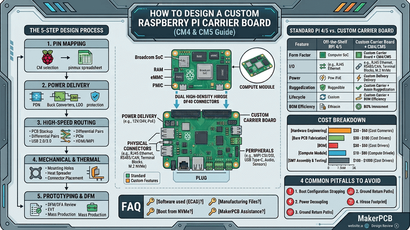
A custom Raspberry Pi carrier board (or baseboard) is a dedicated PCB designed to host a Raspberry Pi Compute Module (such as the CM4 or CM5) and route its processing power into application-specific interfaces, power rails, and industrial connectors. Whether you are building an edge AI gateway, an industrial IoT controller, or medical equipment, designing a carrier board allows you to transition seamlessly from a proof-of-concept to a scalable, production-ready embedded product.
This comprehensive guide covers the architecture of Compute Module baseboards, a 5-step engineering and design workflow, cost breakdowns, layout best practices, and DFM (Design for Manufacturability) guidelines.
What Is a Raspberry Pi Carrier Board?
A Raspberry Pi carrier board (also called a baseboard or IO expansion board) is the motherboard onto which a Raspberry Pi Compute Module is mounted.
While standard Raspberry Pi single-board computers (SBCs) come with fixed USB, HDMI, and power ports, a Compute Module contains only the core essentials: the Broadcom SoC (System on Chip), RAM, eMMC flash storage, power management IC (PMIC), and optional wireless circuitry. It exposes all system interfaces via dual high-density Hirose DF40 board-to-board connectors.
The custom carrier board provides the physical and electrical infrastructure for the module:
• Power delivery: Stepping down industrial 12V/24V inputs, PoE (Power over Ethernet), or Li-ion battery supplies.
• Physical connectors: Industrial Ethernet (RJ45/M12), RS485/CAN bus, terminal blocks, M.2 NVMe slots, and USB Type-C.
• Peripherals: Camera (MIPI CSI), Display (MIPI DSI/HDMI), audio codecs, custom sensor arrays, and hardware watchdogs.
Standard Raspberry Pi 4/5 vs. Custom Carrier Board with Compute Module
Using a standard Raspberry Pi 4 or 5 is ideal for prototyping, but commercial products require the reliability, custom footprint, and supply chain control of a Compute Module carrier board.
| Feature / Factor | Off-the-Shelf Raspberry Pi 4/5 | Custom Carrier Board + CM4/CM5 |
| Form Factor & Enclosure | Fixed layout; ports on multiple edges | 100% customized to fit your enclosure dimensions |
| I/O & Connectors | Consumer-grade USB, Micro-HDMI | Screw terminals, M8/M12, locking JST, PCIe M.2 slots |
| Power Architecture | Strict 5V USB-C input | Wide-range DC (9V–36V), PoE (802.3af/at), or battery PMIC |
| Ruggedization | Commercial grade (0°C to 50°C) | Industrial grade (-20°C to +85°C), conformal coating, secure mounting |
| Lifecycle & Supply | Standard consumer lifecycles | Guaranteed availability (typically 7–10+ years for industrial CM) |
| Unit BOM Efficiency | Includes redundant ports and silicon | Stripped of unused components; optimized unit cost at scale |
If you are evaluating architecture for a new commercial product, explore our hardware development guides to understand the full development lifecycle.
The 5-Step Raspberry Pi Carrier Board Design Process
Step 1 — Select the Compute Module & Define Pin Mapping
Choose between the Raspberry Pi CM4 (cost-effective, proven, PCIe Gen 2.0) and the CM5 (higher processing speed, PCIe Gen 3.0, enhanced I/O performance).
• Download the official mechanical drawings and schematic symbols.
• Map all essential interfaces: PCIe, USB 2.0/3.0, Ethernet (RGMII/Gigabit PHY), MIPI CSI/DSI, SPI, I2C, UART, and GPIOs.
• Tip: Create a pin-multiplexing spreadsheet before beginning schematic capture. Raspberry Pi SoCs share functions across specific pins; validating your pin map early avoids schematic respins.
Step 2 — Architect the Power Delivery Network (PDN)
Power integrity is the leading cause of field failures in embedded hardware. The Compute Module requires a stable +5V rail (±5%) with low ripple, capable of supplying up to 3A to 5A peak current depending on processor load and connected peripherals.
• Input Protection: Implement reverse-polarity protection, TVS surge diodes, and over-voltage lockout (OVLO).
• Voltage Regulation: Use high-efficiency synchronous buck converters if stepping down from 12V or 24V industrial rails.
• Peripheral Rails: Route separate, low-noise LDO regulators for sensitive analog audio, camera sensors, or ADC lines.
Step 3 — Route High-Speed Differential Pairs
Compute Modules break out several high-speed interfaces that require a 4-layer or 6-layer PCB stackup with controlled impedance:
• USB 2.0 / USB 3.0: 90Ω differential impedance; intra-pair length matching within 0.15 mm.
• PCIe Lanes (Gen 2 / Gen 3): 100Ω (or 85Ω depending on spec) differential impedance; avoid layer changes where possible. Keep return paths continuous over solid ground reference planes.
• HDMI 2.0 & MIPI CSI/DSI: 100Ω differential impedance; tightly matched trace lengths with zero stubs.
• Layer Stackup Tip: Use a symmetrical stackup (e.g., Signal - GND - Power - Signal for 4-layer, or Signal - GND - Signal - Power - GND - Signal for 6-layer) to suppress crosstalk and pass EMI/EMC compliance tests.
Step 4 — Mechanical Integration & Thermal Dissipation
The carrier board must precisely align with the Hirose DF40C-100DS-0.4V connectors on the Compute Module.
• Mounting Holes: Place four M2.5 mounting standoffs matching the Raspberry Pi CM mechanical specifications.
• Thermal Management: The BCM2711/BCM2712 SoC generates significant heat under sustained computational loads. Design ground copper pours under the module to act as heat spreaders, or ensure clearance for passive/active heatsinks.
• Connector Ergonomics: Place high-frequency connectors (Ethernet, USB) on one board edge to simplify enclosure cutouts and cable routing.
Step 5 — Prototype, DFM Review, and PCBA Manufacturing
Once the schematic and layout pass electrical rule checks (ERC) and design rule checks (DRC), prepare manufacturing outputs:
1. DFM Review: Run Design for Manufacturability and Design for Assembly (DFA) checks to ensure solder mask dams, trace spacing, and pad geometry align with standard SMT lines.
2. Engineering Validation Tests (EVT): Order an initial prototype batch (5 to 20 units) to validate boot sequences, power rail ripple under load, high-speed interface signal integrity, and peripheral drivers.
3. Mass Production: Scale up using automated Pick-and-Place, SMT reflow, 3D Automated Optical Inspection (AOI), and custom functional test jigs.
MakerPCB’s turnkey manufacturing services handle PCB fabrication up to 32 layers and fine-pitch component placement down to 0.35 mm, delivering tested carrier boards directly to your assembly line.
Cost Breakdown: Custom Carrier Board Development
The total cost to develop and manufacture a carrier board includes one-time engineering (NRE) and unit production costs.
| Cost Component | Typical Price Range | Primary Cost Drivers |
| Hardware Engineering (NRE) | 8,000+ | Schematic complexity, layer count, high-speed routing, BSP development |
| Bare PCB Fabrication | 25 per board | Layer count (4 to 8 layers), board size, surface finish (ENIG vs. HASL) |
| BOM (Peripherals + Passives) | 90 per board | Industrial connectors, PMICs, PCIe chips, interface transceivers |
| Compute Module (CM4/CM5) | 95 per unit | RAM configuration (1GB–8GB), eMMC storage size, onboard Wi-Fi |
| SMT Assembly & Testing | 18 per board | Component count, double-sided SMT, automated functional testing (FCT) |
Need an exact budget for your hardware project? Submit your design files via MakerPCB Online Ordering to receive a transparent fabrication and BOM quote.
4 Common Carrier Board Design Pitfalls to Avoid
1. Improper Boot Configuration Strapping: Ensure that the
nEXTRST,GLOBAL_EN, and boot-mode pins (such asnRPIBOOT) are correctly pulled up or down. Failure to configure these pins properly can lock the eMMC or prevent USB flashing.2. Inadequate Power Decoupling on Peripheral Lines: High-power peripherals like 4G/5G cellular modems or NVMe drives cause voltage sags that reset the Compute Module. Add dedicated bulk tantalum or ceramic capacitors near peripheral sockets.
3. Ignoring High-Speed Ground Return Paths: Route differential pairs (USB, PCIe, HDMI) strictly over an unbroken, contiguous ground reference plane. Crossing a plane split introduces impedance discontinuities and severe EMI emissions.
4. Incorrect Hirose Connector Footprint: Always use verified library footprints for the Hirose DF40 board-to-board connectors. Reversing pin orientation is one of the most common causes of complete board respins.
Frequently Asked Questions (FAQ)
What software is used to design a Raspberry Pi carrier board?
Industry-standard ECAD suites such as KiCad, Altium Designer, and Cadence OrCAD/Allegro are widely used. The Raspberry Pi Foundation provides official reference schematics and footprint symbols in both KiCad and Cadence formats.
Can I boot the Compute Module from NVMe SSD on a custom carrier board?
Yes. On both the CM4 and CM5, you can break out the PCIe lane to an M.2 M-Key slot. With updated Raspberry Pi bootloader firmware, the system can boot directly from a high-speed NVMe solid-state drive without requiring an SD card or eMMC.
What files are required to get a manufacturing quote?
To manufacture your carrier board, you need to provide:
1. Gerber / ODB++ files (copper layers, solder mask, silkscreen, drill files).
2. Bill of Materials (BOM) with exact manufacturer part numbers (MPN) and reference designators.
3. Pick and Place / Centroid file (X-Y component coordinates).
4. Fabrication Drawing indicating PCB thickness, layer stackup, impedance targets, and surface finish (ENIG recommended).
How does MakerPCB assist with custom carrier board projects?
MakerPCB provides end-to-end hardware solutions: from initial electronic design services (schematic capture, high-speed PCB layout, firmware support) to PCB fabrication, component sourcing, and SMT assembly.
Conclusion
Designing a custom Raspberry Pi carrier board empowers you to build commercial-grade, compact, and cost-effective embedded systems tailored precisely to your application requirements. By following systematic pinout mapping, strict power delivery design, and controlled-impedance layout standards, you can avoid costly hardware revisions.
Ready to bring your carrier board design to life? Contact the MakerPCB Engineering Team today for design reviews, DFM feedback, and fast-turn prototype fabrication.

{{ commentCount }} Comments