
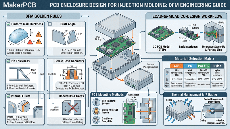
Designing a custom plastic enclosure for a Printed Circuit Board Assembly (PCBA) requires a tight bridge between electrical engineering (ECAD) and mechanical engineering (MCAD). A well-engineered electronic enclosure does more than just look good—it protects sensitive electronics, manages thermal dissipation, provides strain relief for connectors, and is optimized for low-cost, defect-free plastic injection molding.
This guide provides an engineering-grade walkthrough of PCB enclosure design for injection molding, covering Design for Manufacturability (DFM) rules, screw boss geometry, snap-fit mechanics, thermal and ingress protection (IP), and material selection.
Why You Must Design the Enclosure Around the PCB (Not Vice Versa)
The leading cause of costly mold revisions (tooling rework) is designing an aesthetic enclosure shell first and attempting to force-fit the PCBA later.
Always adopt an ECAD-to-MCAD co-design workflow:
1. Export a 3D PCB Model (STEP File): Export the full 3D assembly from your ECAD software (Altium, KiCad, Cadence) including the board outline, connector heights, electrolytic capacitors, heatsinks, and keep-out areas.
2. Lock Interface Faces First: Fix the location of high-stress and user-facing components (USB ports, barrel jacks, pushbuttons, LEDs, and display screens) to establish enclosure openings.
3. Calculate Tolerance Stack-Up: Account for PCB manufacturing tolerance (±0.1 mm to ±0.2 mm), component soldering height variance (±0.3 mm), and plastic molding shrinkage. Always maintain a minimum 1.0 mm to 1.5 mm internal clearance between tall components and the inner enclosure wall.
4. Establish the Parting Line Early: Determine where the core and cavity mold halves separate. Place the parting line along natural aesthetic feature lines to hide witness marks.
7 Golden DFM Rules for Injection-Molded Electronics Enclosures
Injection molding requires molten polymer to flow smoothly through a mold cavity and solidify uniformly. Violating DFM rules results in sink marks, warpage, flash, void formation, and high tooling costs.
| DFM Parameter | Recommended Design Guideline | Engineering Purpose / Risk Avoided |
| Uniform Wall Thickness | 1.5 mm – 3.0 mm (nominal); keep thickness variation under 15% | Prevents non-uniform cooling, internal voids, and severe part warpage. |
| Draft Angle | 1.0° – 2.0° per side on vertical walls (add +1.0° per 0.025 mm of texture depth) | Allows the part to eject cleanly from the mold without drag marks. |
| Rib Thickness | 0.5× to 0.6× of the nominal wall thickness | Provides structural rigidity without causing cosmetic sink marks on outer surfaces. |
| Internal Fillets & Radii | Inside radius: R ≥ 0.5× wall thickness; Outside radius: R ≥ 1.5× wall thickness | Eliminates stress concentration points and improves molten plastic flow. |
| Screw Boss Geometry | Outer Diameter (OD) = 2.0× to 2.4× screw OD; Root thickness = 0.6× wall | Prevents boss hoop-stress rupture and surface sink marks. |
| Undercuts | Minimize or eliminate; use pass-through cores where possible | Reduces mold complexity; avoids expensive mechanical side-actions/lifters. |
| Gate Placement | Near thick sections, away from cosmetic faces | Ensures balanced mold filling; conceals gate vestige marks. |
PCB Mounting Architecture: Bosses, Standoffs, and Snap-Fits
How you secure the board inside the plastic housing dictates assembly labor, mechanical vibration resistance, and serviceability.
1. Self-Tapping Screw Bosses (Most Common)
For plastic housings, thread-forming screws (e.g., Delta PT or Plastite) are standard:
• Hole Diameter: Approximately 0.8× of the screw's nominal diameter.
• Gussets & Ribs: Never attach a tall, freestanding boss directly to a flat wall. Connect bosses to adjacent side walls using supporting gussets (thickness ≈ 0.6× wall thickness) to withstand driving torque.
• PCB Keep-Out: Maintain a minimum 1.0 mm annular keep-out ring around PCB mounting holes. Keep copper traces, vias, and SMT pads outside this area to avoid short circuits from the screw head.
2. Threaded Brass Heat-Set Inserts
If the enclosure will be opened frequently for maintenance or battery replacement, use ultrasonic or heat-staked brass threaded inserts. They provide reusable, high-torque metal-on-metal threads (M2, M2.5, M3) that prevent plastic thread stripping.
3. Cantilever Snap-Fit Joints
For high-volume consumer devices requiring toolless, rapid assembly:
• Use tapered cantilever hooks to distribute strain evenly along the beam.
• Keep maximum strain below the allowable limit of the resin (typically under 1% to 2% for ABS).
• Add guide ribs inside the housing to align the PCB before the snap-fits engage.
Thermal Management & Ingress Protection (IP Rating)
Managing Heat in Plastic Housings
Unlike aluminum, plastic resins are thermal insulators (low thermal conductivity, k ≈ 0.1 to 0.3 W/m·K).
• Ventilation Slots: Add convection slots directly above and below heat-generating components (PMICs, SoCs, MOSFETs). Keep vent slot widths below 2.5 mm to prevent accidental finger contact with live circuits (IEC 62368 compliance).
• Integrated Heat Spreaders: Use thermal pads (TIM) to bridge heat from high-power ICs directly to an external aluminum faceplate or internal copper heat sinks.
Designing for Dust & Water Ingress (IP54 to IP67)
If your product requires outdoor or industrial sealing:
• Tongue-and-Groove Joint: Implement a perimeter tongue-and-groove joint between the top and bottom enclosure halves.
• Elastomer Gaskets / O-Rings: Compress a continuous silicone or EPDM gasket (minimum 25% to 30% nominal compression) inside the groove.
• Overmolding (2K Injection Molding): For high-end waterproof products, chemically bond a soft TPE/TPU seal directly onto the rigid housing during molding.
Selecting the Right Enclosure Plastic Resin
Selecting the appropriate polymer grade depends on mechanical strength, operating temperature, flammability standards, and cosmetic finishing requirements.
| Plastic Material | Mechanical Properties | Thermal & UV Resistance | Flammability & Certifications | Best Used For |
| ABS | High impact strength, easy to mold, low cost | Heat deflection: ~80°C; poor outdoor UV resistance | Standard UL94 HB (UL94 V-0 grades available) | Consumer electronics, IoT sensors, indoor housings |
| Polycarbonate (PC) | Extremely high impact strength, optically clear | Heat deflection: ~130°C; good UV resistance | Inherent flame retardancy (UL94 V-0 easily achieved) | Industrial equipment, rugged handhelds, transparent light pipes |
| PC + ABS Blend | High impact, excellent stiffness, fine surface finish | Heat deflection: ~100°C to 115°C; moderate UV | UL94 V-0 commonly available | Automotive electronics, telecommunication gateways, medical devices |
| Nylon (PA6 / PA66) | Extreme wear resistance, chemical resistance | Heat deflection: ~150°C+; absorbs moisture | UL94 V-2 to V-0 | Under-the-hood automotive, harsh chemical environments |
EMI/EMC Tip: If your PCBA must pass strict FCC/CE radiation limits and cannot be shielded on-board, specify conductive inner-wall coatings (such as selective vacuum metallization, nickel conductive paint, or internal sheet metal shielding cans).
From Rapid Prototype to Injection Mold Tooling: 5 Stages
1. Functional Prototyping (SLA / SLS / CNC): Produce 1:1 physical prototypes. Fit-check real PCBAs, test connector insertions, verify snap-fit deflections, and conduct drop tests.
2. Tooling DFM & Moldflow Analysis: Simulate melt front advancement, identify weld lines (knit lines), verify air vent locations, and confirm uniform cooling.
3. Tooling Fabrication:
• Rapid Aluminum Tooling: 500 – 5,000 shots (ideal for market validation and pilot runs).
• Hardened Steel Tooling (P20 / H13 / S136): 100,000 to 1,000,000+ shots (for long-term high-volume mass production).
4. T1 Samples & First Article Inspection (FAI): Measure initial molded parts with CMM (Coordinate Measuring Machines) against critical 2D drawing tolerances. Conduct complete PCBA assembly tests.
5. Mass Production & Surface Finishing: Ramp production with automated injection cycles, followed by optional pad printing, laser etching, painting, or textured spark finishes (SPI / VDI standards).
By combining custom PCB manufacturing, SMT assembly, injection mold tooling, and final box build assembly under one roof, MakerPCB eliminates the common friction and finger-pointing between board fabricators and plastic molders.
Frequently Asked Questions (FAQ)
What is the minimum wall thickness for an electronic enclosure?
For standard ABS and PC-ABS enclosures, the recommended minimum wall thickness is 1.5 mm. For smaller, handheld consumer gadgets, walls can be reduced to 1.2 mm using high-flow resins, provided adequate structural ribs are added.
How much draft angle should I apply to side walls?
Apply a minimum of 1.0° of draft per side for smooth surfaces. If your exterior has a textured finish (such as VDI 3400 or Mold-Tech textures), add an additional 1.0° to 1.5° of draft per 0.025 mm (0.001 in) of texture depth to prevent scuff marks during mold ejection.
How do I prevent sink marks near screw bosses?
To eliminate sink marks on cosmetic surfaces:
1. Do not let the boss wall thickness exceed 60% of the adjacent main wall thickness.
2. Core out the base of the boss.
3. Use connecting gussets rather than a single solid thick pillar of plastic.
Can MakerPCB assist with both mechanical enclosure design and PCB assembly?
Yes. MakerPCB provides comprehensive electronic and mechanical design services as well as turnkey manufacturing. Our engineering team ensures your board layout, mechanical clearances, mold tooling, and system testing are synchronized from day one.
Conclusion
A successful plastic PCB enclosure requires balancing mechanical durability, thermal dissipation, electrical interface clearances, and strict injection molding DFM guidelines. By designing around the board outline, enforcing uniform wall thicknesses, and incorporating robust boss and rib geometry, you can avoid expensive mold modifications and launch your product on schedule.
Ready to manufacture your electronic product? Upload your 3D CAD and PCB Gerber files to MakerPCB for an instant DFM engineering review and mold tooling quotation.

{{ commentCount }} Comments