
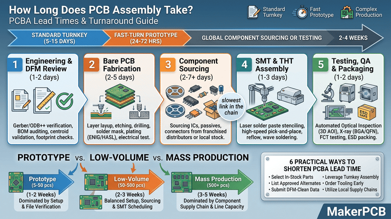
For most standard turnkey projects, PCB assembly lead time ranges between 3 and 15 business days. A fast-turn prototype with in-stock components can ship in as little as 24 to 72 hours, while complex production runs involving global component sourcing or extensive functional testing typically take 2 to 4 weeks.
Understanding the PCB Assembly (PCBA) timeline—and knowing where bottlenecks occur—is essential for keeping hardware development on schedule. This guide breaks down the lead times for each manufacturing stage, compares prototype vs. mass production timelines, and explains actionable ways to expedite your order.
Quick Summary: PCB Assembly Timeline by Stage
A complete turnkey PCBA order consists of five sequential steps. The total lead time is dictated by the slowest link in the chain (usually component procurement).
| Production Stage | Standard Turnaround | Quick-Turn / Expedited | Key Activities & Critical Paths |
| 1. Engineering & DFM Review | 1 – 2 days | 4 – 12 hours | Gerber/ODB++ verification, BOM auditing, centroid validation, footprint checks. |
| 2. Bare PCB Fabrication | 2 – 5 days | 24 – 48 hours | Layer layup, etching, drilling, solder mask, plating (ENIG/HASL), electrical test. |
| 3. Component Sourcing | 2 – 7+ days | 24 – 48 hours (in-stock) | Sourcing ICs, passives, connectors from franchised distributors or local stock. |
| 4. SMT & THT Assembly | 1 – 3 days | 12 – 24 hours | Laser solder paste stenciling, high-speed pick-and-place, reflow, wave soldering. |
| 5. Testing, QA & Packaging | 1 – 2 days | 4 – 12 hours | Automated Optical Inspection (3D AOI), X-ray (BGA/QFN), FCT testing, ESD packing. |
| Total Turnkey Lead Time | 5 – 15 days | 3 – 5 days | Door-to-door transit adds 2–4 days via DHL/FedEx/UPS. |
Prototype vs. Low-Volume vs. Mass Production Lead Times
The size and purpose of your PCB assembly order directly dictate which stage dominates the timeline:
1. Prototype PCBA (5 to 50 Boards)
• Typical Lead Time: 1 to 2 weeks (Expedited: 3 to 5 business days).
• Characteristics: Machine setup, SMT feeder calibration, and DFM validation represent the largest percentage of effort. SMT lines spend more time being configured than actually placing components.
2. Low-Volume Assembly (50 to 500 Boards)
• Typical Lead Time: 2 to 3 weeks.
• Characteristics: Balanced workflow. Component availability is the primary factor. Panels run continuously on SMT lines once feeders are verified.
3. High-Volume Mass Production (500 to 10,000+ Boards)
• Typical Lead Time: 3 to 6 weeks.
• Characteristics: Component reel procurement and manufacturing line scheduling dominate. Dedicated test jigs, In-Circuit Testing (ICT), and conformal coating cycles add incremental time.
Turnkey PCBA vs. Consigned (Kitted) Assembly: Impact on Lead Time
How you supply components fundamentally affects project turnaround:
• Turnkey PCBA (Recommended for Speed): The manufacturer fabricates the bare PCB and procures all BOM components simultaneously. Overlapping fabrication and sourcing saves 3 to 7 business days.
• Consigned / Kitted Assembly: You source parts and ship them to the assembler. Delays in kit preparation, international customs clearance, part miscounts, or damaged component reels can stall production lines for weeks.
The Top 5 Factors That Delay PCB Assembly
If a PCBA order is delayed, it almost always traces back to one of the following root causes:
1. Component Lead Times & Allocation: Certain specialized microcontrollers (MCUs), PMICs, or RF modules may have 12-to-26-week factory lead times.
2. BOM (Bill of Materials) Ambiguities: Incomplete Manufacturer Part Numbers (MPNs), missing package codes (e.g., specifying "0603 resistor" without tolerance or voltage rating), or obsolete parts require back-and-forth email confirmations.
3. DFM & Footprint Mismatches: Errors caught during Design for Manufacturability reviews—such as mismatched pad sizes, reversed diode polarities, or missing centroid (X-Y) coordinates—halt production until corrected.
4. Complex Packaging & High-Density Interconnects: Boards featuring fine-pitch BGAs (down to 0.35 mm pitch), ultra-dense 01005 passives, or QFNs require mandatory 3D X-ray inspection (AXI), which extends QA test cycles.
5. Custom Functional Testing (FCT): Elaborate functional test routines requiring custom programming fixtures, burn-in chambers, or RF calibration add 1 to 3 days to final validation.
6 Practical Ways to Shorten Your PCB Assembly Lead Time
To ensure your boards ship in the fastest possible timeframe:
1. Select In-Stock, Standard Components: Design using active, high-inventory parts from major suppliers (Yageo, Murata, TI, STMicroelectronics, Microchip) rather than single-source, obscure ICs.
2. List Approved Alternates (AML / AVL): Provide secondary and tertiary acceptable manufacturer part numbers directly in your BOM so sourcing teams can substitute parts immediately without waiting for approval.
3. Submit a DFM-Clean Data Package: Ensure your release bundle contains complete Gerber/ODB++ files, an audited BOM with exact MPNs, a centroid (Pick-and-Place) file, and clear assembly drawings with component polarities clearly marked.
4. Leverage Turnkey Assembly: Use a single manufacturing partner to handle PCB fabrication, parts procurement, and assembly concurrently.
5. Order Pre-Production Tooling Early: For production batches, prepare custom solder stencils and test fixtures during the PCB fabrication phase.
6. Utilize Local Supply Chains: Partner with manufacturers with immediate access to massive electronics markets (such as Shenzhen), where hard-to-find components can be delivered same-day.
Why MakerPCB Delivers Faster Turnaround Times
Headquartered in Shenzhen—the core of the global electronics ecosystem—MakerPCB dramatically compresses PCBA lead times:
• Same-Day Local Sourcing: Components that take weeks to ship through global distributors can often be sourced from verified local supply channels in 24 to 48 hours.
• Unified Manufacturing: Bare PCB fabrication, component procurement, SMT assembly, and box build electromechanical integration are handled under one roof, eliminating vendor handoff delays.
• Real-Time Transparency: Track your production milestones from BOM auditing to SMT placement via our online ordering and tracking platform.
Frequently Asked Questions (FAQ)
How long does bare PCB fabrication take without assembly?
Standard 2-layer to 6-layer rigid PCBs take 2 to 4 business days for prototype runs. Quick-turn bare board services can produce 2-layer boards in 24 hours. Complex multilayer boards (10+ layers, HDI, blind/buried vias) take 5 to 8 business days.
When does the lead time clock officially start?
The official lead time begins after the DFM engineering review is approved and all BOM components have arrived at the assembly facility, not the moment the order is paid online. Ensuring your design files are error-free prevents initial clock delays.
Can SMT assembly be completed in 24 hours?
Yes. If bare boards and all BOM components are pre-kitted and in stock, the physical SMT placement, reflow soldering, and AOI inspection for a small prototype batch can be completed in 24 to 48 hours via quick-turn expedited services.
Does PCB surface finish affect assembly lead time?
Standard finishes like HASL (Lead-Free) and ENIG (Electroless Nickel Immersion Gold) are processed in standard cycles. Specialized finishes like Hard Gold, Immersion Silver, or ENEPIG may add 1 to 2 days to the bare board fabrication phase.
Conclusion
PCB assembly lead time is governed primarily by component sourcing and DFM preparation, rather than the physical soldering process. By cleaning your BOM, providing approved alternates, and choosing a turnkey manufacturing partner with deep supply chain integration, you can reliably shorten delivery times from weeks to days.
Need fast, reliable PCB assembly for your next project? Upload your Gerber files and BOM to MakerPCB or contact our engineering team for an instant quote and firm lead-time commitment.

{{ commentCount }} Comments